× close
It is a common hack to stretch a balloon out to make it easier to inflate. When the balloon stretches, the width crosswise shrinks to the size of a string. Noah Stocek, a Ph.D. student collaborating with Western physicist Giovanni Fanchini, has developed a new nanomaterial that demonstrates the opposite of this phenomenon.
Working at Interface Science Western, home of the Tandetron Accelerator Facility, Stocek, and Fanchini formulated two-dimensional nanosheets of tungsten semi-carbide (or W2C, a chemical compound containing equal parts of tungsten and carbon atoms), which, when stretched in one direction, expand perpendicular to the applied force. This structural design is known as auxetics.
The trick is that the structure of the nanosheet itself isn’t flat. The atoms in the sheet are made of repeating units consisting of two tungsten atoms for every carbon atom, which are arranged metaphorically like the dimpled surface of an egg carton. As tension is applied across the elastic nanosheet in one direction, it expands out in the other dimension as the dimples flatten.
× close
Prior to this innovation, there was only one reported material that could expand by 10% per unit length in this counter-intuitive way. The Western-engineered tungsten semi-carbide nanosheet can expand to 40%, a new world record.
“We were specifically looking to create a two-dimensional nanomaterial from tungsten semi-carbide,” said Stocek. “In 2018, theorists predicted that it might exhibit this behavior to an excellent level, but nobody had been able to develop it, despite extensive attempts by research groups all over the world.”
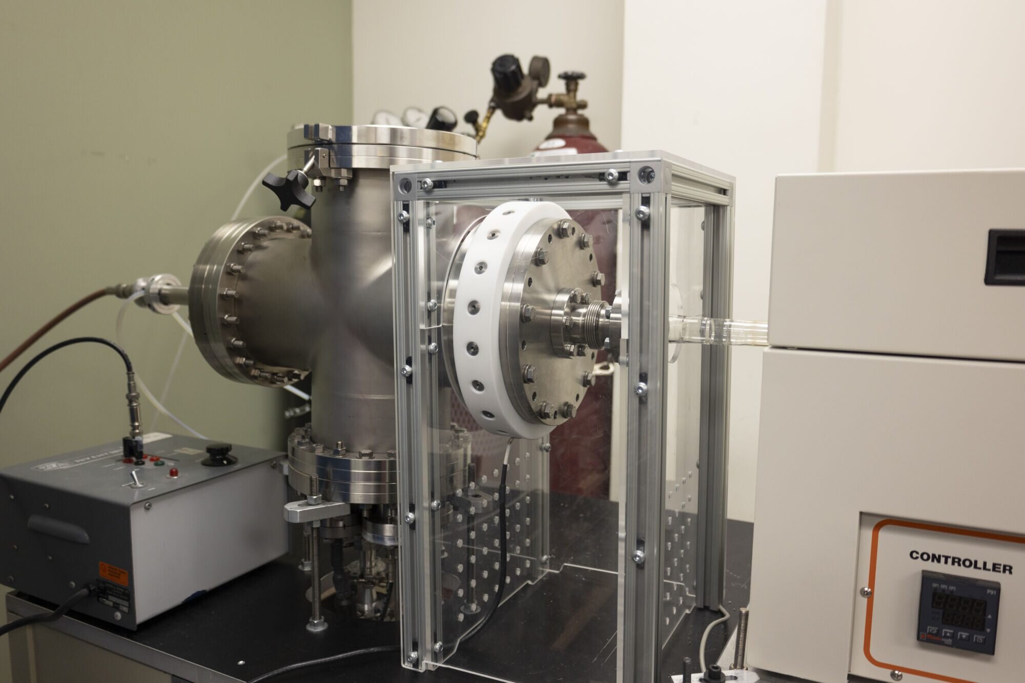
It wasn’t possible to construct the new tungsten semi-carbide nanomaterial using chemical means, so Stocek and Fanchini relied on plasma physics to form the single-atom layers. Made of charged particles of atoms, plasma is the fourth state of matter (with solid, liquid, and gas). Plasma can be observed in the natural world in the northern lights, or Aurora Borealis, and the sun’s corona during the recent solar eclipse. It is also used in neon lighting, fluorescent tubes, and flat-screen TVs.
Typically, the instrumentation used to make two-dimensional nanomaterials is special furnaces where gases are heated at a high enough temperature to react and form the desired substance chemically. This approach simply did not work because any chemical reaction, the most common process, would lead to a product different from the desired nanomaterial.
“That’s where most researchers who tried to get this material before us got stuck, so we had to pivot,” said Fanchini.
Instead of heating a gas made of tungsten and carbon atoms in furnaces, which would produce neutral particles as you would get for solids, liquids, or gases, Stocek and Fanchini designed a new customized instrumentation that produces a plasma, which is made up of electrically charged particles.
× close
Stretch goals
There are countless possible applications for these W2C nanosheets, beginning with a new type of strain gauge. These commercially available gauges are a standard way to measure expansion and stretch in everything from airplane wings to household plumbing.
“Imagine if you want to know if a pipe in your house is deforming and risks bursting at some point. You can stick a sensor on the pipe made from this two-dimensional nanomaterial and then use a computer to monitor the current passing through it. If the current rises, it means the pipe is expanding and risks bursting,” said Stocek.
The new nanomaterial, in fact, becomes more electrically conductive, and that opens the door for endless possibilities to use in things like sensors or any device that detects events or changes in the environment and sends the information to other electronics. Another application is embedding the material right in stretchable electronics, like wearable technology so that they have more conductivity.
“Normally, strain gauges would rely on the fact that when you stretch a material, it gets thinner, and you change the conductivity of a material to carry a current,” said Fanchini. “With this new nanomaterial, this would no longer be the case.”
The findings are published in the journal Materials Horizons.
More information:
Noah B. Stocek et al, Giant Auxetic Behavior in Remote-plasma Synthesized Few-Layer Tungsten Semicarbide, Materials Horizons (2024). DOI: 10.1039/D3MH02193A

Daisy Hips is a science communicator who brings the wonders of the natural world to readers. Her articles explore breakthroughs in various scientific disciplines, from space exploration to environmental conservation. Daisy is also an advocate for science education and enjoys stargazing in her spare time.